
Nanotechnology for the environment and future sensors
With advanced nanotechnology, researchers from Halmstad and Lund are developing pioneering components that can be used in several areas. For example, the technology can be used for smart monitoring, desalination and purification of seawater, and energy storage.
“We have found a unique solution to the big problem of electrical leakage along the pixel surfaces. This will lead to significantly lower power consumption in the camera sensor and thus more competitive sensor systems.”
Håkan Pettersson, Professor of Physics
At Halmstad University, advanced development of new hardware based on nanotechnology has been conducted for many years. Together with researchers at NanoLund, the research group, led by Håkan Pettersson, Professor of Physics at Halmstad University, develops new nanomaterials and components for future optical sensor systems and clean technology. In three ongoing projects, the research group collaborates with Linköping University, Harvard University in USA, Central University of Rajasthan in India and the company IRnova.
“In the project Bias-tunable quantum disc-in-nanowire photonic crystal IR detectors, funded by the Swedish Research Council, we have now developed a unique nanosensor where the optical properties can be controlled with an electrical signal”, says Håkan Pettersson.
Håkan Pettersson is Professor of Physics at the School of Information Technology at Halmstad University.
Millions of nanowires amplify the signal
The sensor consists of several million interconnected nanowires of the material indium phosphide (InP) with embedded thin quantum segments of indium arsenide phosphide (InAsP). According to Håkan Pettersson, this makes the sensor extremely sensitive to both visible light and infrared (IR) light. The nanowires have a thin electrically conductive shell around them, called a wrap-gate. By connecting an electrical signal to this wrap gate, the optical properties of the sensor, such as the sensitivity to different wavelengths, can be adapted and controlled in a new way.
“The sensor will now be further developed by embedding the nanowires in an optical crystal that significantly enhances the signal strength further”, says Håkan Pettersson.
The developed sensors have a wide range of applications in many different applications such as monitoring, communication, quality control and medicine.
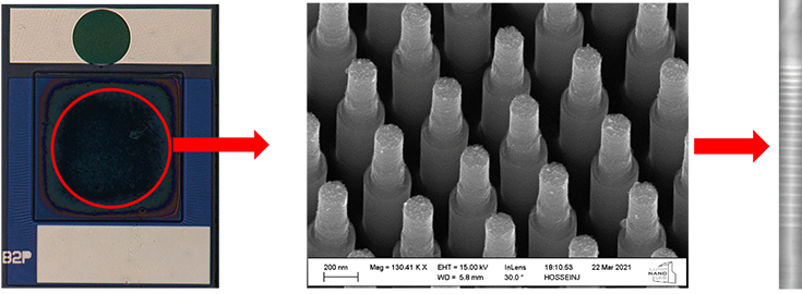
To the left is an optical sensor with various contacts seen from above. The red ring indicates an active sensor surface (approx. 1 mm2). In the middle, the image is taken with an electron microscope with 130,000 times magnification. The processed nanowires are clearly visible. To the right is an electron microscope image of a nanowire showing the embedded quantum segments as a white barcode.
Unique solution for more efficient sensors
In the project Superlattice-based HOT MWIR imaging sensors, funded by Vinnova, Håkan Pettersson's research group, together with the company IRnova has drastically improved the properties of commercial sensor chips based on superlattices. The superlattices consist of hundreds of extremely thin layers, just a few nanometres thick, of alternating indium arsenide (InAs) and gallium antimonide (GaSb). The layers are grown on top of each other and are connected according to the laws of quantum physics to a completely new optical material with tailored electrical and optical properties.
“We have found a unique solution to the big problem of electrical leakage along the pixel surfaces. This will lead to significantly lower power consumption in the camera sensor and thus more competitive sensor systems, says Håkan Pettersson, and continues:
“In a related project, where we recently applied for research funding, the goal is to design complex 3D metal structures in nanoscale on each pixel surface. They are called optical meta-surfaces and are used to capture the IR light in the pixels efficiently. This dramatically increases the efficiency of the sensor while minimising the IR leakage between pixels.”
The developed sensor systems have a large use in safety, thermal imaging, environmental monitoring and medicine.
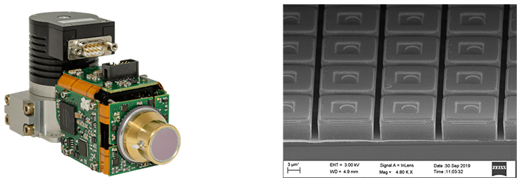
To the left is a complete superlattice camera with electronics and Stirling cooler to cool down the built-in image sensor chip to -130 ° C. To the right is an electron microscope image of the pixels on the image sensor chip.
Nanotechnology to purify water
Before the summer, PhD student Ebrahim Chalangar, defended his doctoral thesis “Synthesis and Characterisation of ZnO / Graphene Nanostructures for Electronics and Photocatalysis”. In his thesis, he developed new composite materials of super-thin carbon layers, also called graphene, combined with various nanostructures of zinc oxide (ZnO). The research was funded by Ångpanneföreningen (ÅForsk) and the Knowledge Foundation. The composite materials can be used for 3D printing of electronics, photocatalytic purification and desalination of seawater for drinking water.
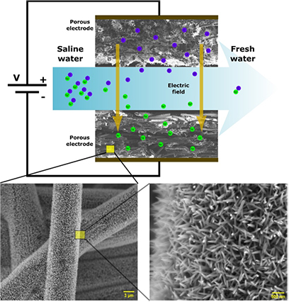
The top picture shows the desalination component itself with two porous electrodes. A voltage source is connected between the electrodes. The electric field that arises separates positive Na ions and negative Cl ions in the seawater, which are absorbed by the respective electrode. Below are two electron microscope images of the electrode's carbon fibre structure (left) and nanowires on the surface of the fibres (right).
For water desalination, the research group has developed a product that consists of two porous electrodes. The electrodes are made up of carbon fibre networks lined with super-thin nanowires of ZnO. Effectively, the electrodes separate and bind positive sodium ions and negative chlorine ions (sea salt is sodium chloride, NaCl) in flowing saltwater that passes between the electrodes. Other researchers at the University are also participating in this project.
“The technology is very interesting and promising. We are now working with similar technology to develop cheaper, safer and lighter batteries and supercapacitors for energy storage”, says Håkan Pettersson.
Text: Anna-Frida Agardson
Picture: Ida Fridvall
Graphics: Håkan Pettersson
About nanotechnology and nanowires
Nanowires have a typical length of a few micrometres (1 micrometre = 1 millionth of a meter), while the diameter varies from a few nanometers (1 nanometer = 1 billionth of a meter) to several hundred nanometres. Due to the small size and the ability to control different materials on an atomic scale, nanotechnology is often described as “atomic craft” - designing materials at the atomic level. The properties of the nanowires can be varied depending on the material composition, diameter and length.
What makes nanotechnology so special is that substances behave differently at the nano level than they do on a larger scale. Our usual physical laws often no longer apply but are replaced by quantum physics. For example, the electrons in the small embedded InAsP segments, as described above (see microscope images), behave like a wave controlled by quantum mechanical layers. The segments are therefore called quantum discs. By optimising the thickness of the segments, one can tailor their electrical and optical properties. In another work recently submitted to a world-leading journal, researchers have for the first time succeeded in creating internal optical resonances in single quantum disks with light of very long wavelength, which opens up the possibility of using the same nanowires to make extremely “broadband” detectors that are sensitive to very large wavelength ranges. In yet another work, they have created the first nanowire detectors with an internal amplifier in the form of another segment of material fully integrated at one end of the nanowire.
Other advantages of nanoparticles, such as nanowires, are that they have a very large surface area in relation to their volume. This is of great importance for the manufacture of, for example, new types of biosensors. Nanotechnology is already used in a number of different application areas of biology, physics and chemistry, for example, in the development of new materials, electronics, medicine, biotechnology and energy technology.
1 nm = 0.00000000001 m
A human hair is about 50,000 nanometres thick.
Sources: The Nobel Museum, the Foundation for Strategic Research and SwedNanoTech.
How to make nanowires
Researchers start by creating a pattern of small gold particles on the surface where they want the nanowires to grow (usually on a chip or wafer). The chip is then heated in a special kind of oven. Gases are introduced to provide the elements needed for building the different layers in the nanowires. For InP and InAsP nanowire segments, indium, arsenic and phosphorus are used. Gold catalyses the growth of the nanowires, and a single nanowire grows up underneath each gold particle. The bright object at the right-hand end of the nanowire in part c) of the figure above the gold particle used to grow it.
Different materials can be grown in sequence by changing the gases being used. Fast switching permits incredibly thin layers to be grown, creating quantum discs along the axis of the cylindrical wire. Nanowire growth is a relatively simple process because the atoms building the structure self-organise, and automatically find their correct places in the overall structure.
