
Reinventing optical sensors with nanotechnology
Nanotechnology allows us to combine materials with different optical properties in entirely new ways. Components can be made smaller, cheaper and more energy-efficient than those we use today, and new capabilities can be introduced. Researchers from Halmstad and Lund have created unique nanowires that are expected to initiate a new generation of innovative solar cells and light-sensitive detectors, allowing direct integration with conventional silicon-based devices.
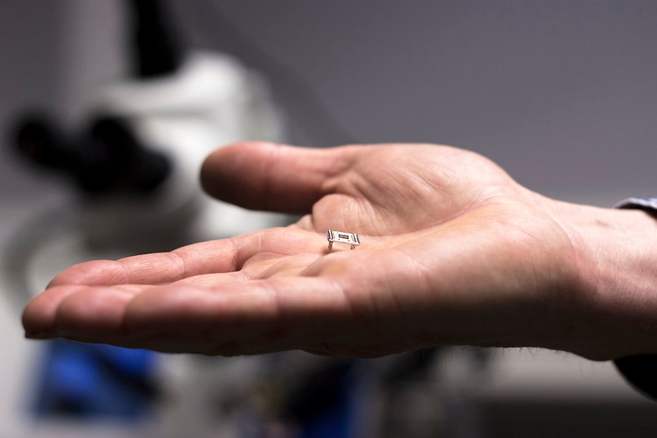
A 'chip carrier' (the rectangular white plate) with the dark semiconductor sample at its centre. Nanowires are held on the semiconductor surface, connected by gold threads to the terminals of the chip carrier. The connections are used to measure the nanowire's properties.
Håkan Pettersson, Professor of Physics at Halmstad University, explains the recent breakthrough:
”We have succeeded in building extremely high-quality, layered structures at the nanometer scale. The layers are of two materials that have different optical properties, which usually makes them incompatible with each other – it's a bit like trying to build with a mixture of Lego and Duplo bricks.”
Catching more rays
The researchers solved the incompatibility by growing the material layers inside needle-like structures called nanowires. The wires have very small diameters, which dramatically reduces the stress built up between the layers, so cracks and other material defects are less likely to occur.
”Heterostructure nanowires with this 'sandwich' structure, make it possible to combine materials with completely different properties. By choosing the right combinations, we can customise nanowires for different applications. Our focus in this project is to develop nanowires for photodetectors. Also, because the diameters of our nanowires are so small, we should be able to grow them directly on a silicon wafer, alongside CMOS* circuitry, which opens the door to new types of integrated optoelectronics”, says Håkan Pettersson.
At the most basic level, a photodetector or solar cell converts light into an electrical signal. By using several million heterostructure nanowires working in parallel, these new devices can be made extra-sensitive to light. They also work over a broader range of wavelengths than is possible with today's technology. Both benefits mean more light can be captured, making these kinds of photodetectors and solar cells more energy efficient.
A leading-edge nanotechnology consortium
The research group at Halmstad University is part of the School of Information Technology, and consists of PhD students Mohammad Karimi, Vishal Jain and Laiq Hussain, and Professor Håkan Pettersson. Håkan Pettersson is also in charge of the Rydberg Core Laboratory (RCL), part of the Rydberg Laboratory of Applied Science (RLAS) research environment, at Halmstad University's School of Business, Engineering and Science.
The group has a longstanding collaboration with NanoLund at Lund University, one of Europe's leading cross-disciplinary consortiums in nanotechnology. Halmstad researchers use the clean-rooms at Lund (Lund NanoLab) to make their devices, before performing electrical and optical measurements in RCL at Halmstad University. The group's research on heterostructure nanowire photodetectors was published in the leading journal Nano Letters in June: 'Room-temperature InP/InAsP Quantum Discs-in-Nanowire Infrared Photodetectors'.
Håkan Pettersson has also recently been selected as Sweden's only representative in the semiconductor physics section of the IUPAP, the International Union of Pure and Applied Physics.
Text: Louise Wandel
Photo: Ida Fridvall
* CMOS (complementary metal-oxide semiconductor) is one of the main techniques for making integrated circuits. CMOS chips are found in almost all modern electronic devices, including camera sensors and computer CPUs.
Read more
NanoLund External link, opens in new window.
International Union of Pure and Applied Physics (IUPAP) External link, opens in new window.
How to make nanowires
Researchers start by creating a pattern of small gold particles on the surface where they want the nanowires to grow (usually on a chip or wafer). The chip is then heated in a special kind of oven. Gases are introduced to provide the elements needed for building the different layers in the nanowires. For InP and InAsP nanowire segments, indium, arsenic and phosphorus are used. Gold catalyses the growth of the nanowires, and a single nanowire grows up underneath each gold particle. The bright object at the right-hand end of the nanowire in part c) of the figure above the gold particle used to grow it.
Different materials can be grown in sequence by changing the the gases being used. Fast switching permits incredibly thin layers to be grown, creating quantum discs along the axis of the cylindrical wire. Nanowire growth is a relatively simple process because the atoms building the structure self-organise, and automatically find their correct places in the overall structure.
